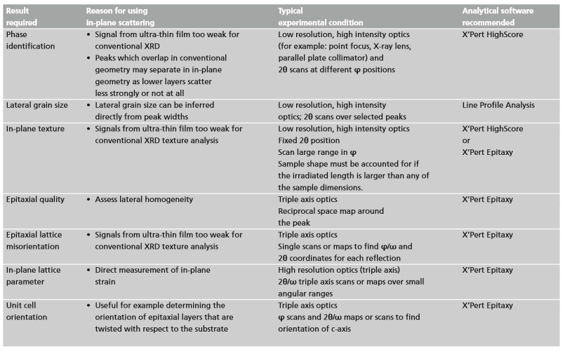
This application note provides a basic introduction to in-plane diffraction. It includes a short description of the technique and demonstrates its application on the X’Pert3 MRD.
Many different in-plane diffraction experiments are possible on the X’Pert3 MRD system, incorporating different types of scan and using different PreFIX optical modules. Examples of different types of experiment are described in this note together with practical tips highlighting the specific areas of concern in in-plane diffraction.
Many different in-plane diffraction experiments are possible on the X’Pert3 MRD system, incorporating different types of scan and using different PreFIX optical modules. Examples of different types of experiment are described in this note together with practical tips highlighting the specific areas of concern in in-plane diffraction. Two examples of in-plane applications are given: Example 1 shows a typical data collection process for a polycrystalline Co thin film. Example 2 shows typical data collection for a single crystal GaN epitaxial lateral overgrowth (ELOG) thin film.
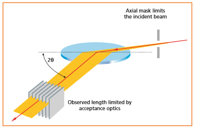
In-plane diffraction refers to the diffraction technique where the incident and diffracted beams are both nearly parallel to the sample surface (see Figure 1). There are two major features of this technique.
Firstly, because the beam is incident at a grazing angle, the penetration depth of the beam is limited to within about 100 nm of the surface. In common with the techniques of GIXRR (Grazing Incidence X-Ray Reflectometry) and GIXRD (Grazing Incidence X-Ray Diffraction) it is used to examine surface layers.
Secondly, the in-plane method measures diffracted beams which are scattered nearly parallel to the surface, and hence measures diffraction from planes that are perpendicular to the sample surface. These planes are inaccessible by other techniques. The position, shape and intensity of Bragg peaks in this geometry can be used for phase identification of thin surface layers and provides information about in-plane texture. Examination of the shapes of these peaks may provide structural information, such as lateral grain size.
Figure 1. Schematic representation of in-plane diffraction
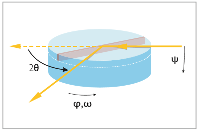
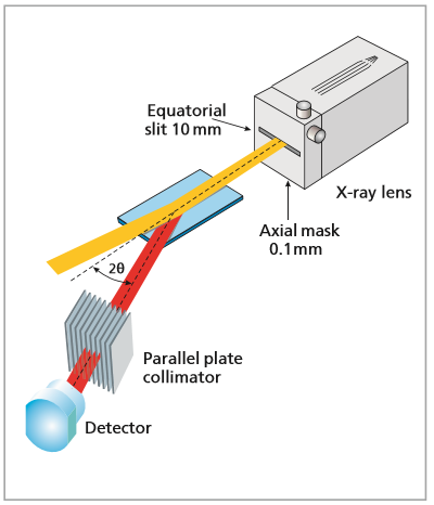
In-plane diffraction can be performed on an X’Pert3 MRD system adapted for in-plane diffraction using standard PreFIX optical components. The X'Pert3 MRD must be initially configured so that the Ω axis can move to –90°. The Ψ axis is set to 90° and the system is ready for in-plane measurements.
The photograph shows the in- plane setup. The angle of incidence onto the surface of the sample is controlled by the Ψ rotation. The in-plane scattering angle is determined by the 2θ angle. The sample can be rotated using φ for large rotations and ω for small rotations (typically up to 2°). Various parallel beam optical configurations can be used for the in-plane technique. The most common configuration for thin film polycrystalline samples is with the X-ray lens which includes a crossed-slits collimator, for the incident beam, and a 0.27° parallel plate collimator on the diffracted beam side.
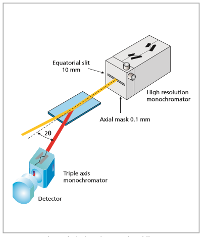
Alternatively, for single crystal or highly textured layers a high resolution monochromator which includes a crossed-slits collimator can be used for the incident beam in conjunction with a rocking curve attachment or a triple axis attachment on the diffracted beam side. Other possibilities are a crossed slits collimator, or a monocapillary at the incident beam side, used in conjunction with a parallel plate collimator and a diffracted beam monochromator at the diffracted beam side.
Sample alignment
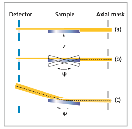
It is important to set the sample so that the beam is incident at an angle close to (slightly larger than) the critical angle for reflection. A procedure to find this position is shown in Figure 2.
With the detector (2θ) at zero (use an attenuator) and with the equatorial crossed slit set to a small value, e.g. 0.1 mm, raise the sample in the Z direction until it cuts the beam intensity to < 50% (a). Scan in ψ (b) to obtain a scan as in Figure 3.
Set the ψ position to an angle just beyond the critical edge for total external reflection (c).
Figure 2. Sample alignment procedure
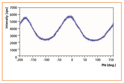
The ψ scan shown in Figure 3 is an example in which ψ is set for a single crystal silicon sample. (The scan is similar to a very low resolution reflectometry scan). Because there are no vertical beam masks, there may be contributions from both the direct beam and totally externally reflected X-rays. The critical edge is the point at which this intensity starts to drop rapidly. As ψ is increased beyond this angle, X-rays penetrate further into the sample. For in-plane diffraction, the angle of incidence,
ψ, should be set at an angle which optimizes the penetration depth. Rays entering at an angle in excess of approximately 1.4 times the critical angle are not able to exit the material. This provides an upper limit for the angle of incidence. The ideal angle of incidence will therefore fall between the critical angle and approximately 1.4 times the critical angle. As a general guide set the angle of incidence just beyond the critical angle, somewhere within the region with the most rapid intensity drop. After an in- plane Bragg peak has been found (away from the direct beam) the y position can be optimized again for maximum intensity.
An in-plane Bragg peak can be found by scanning in 2θ, for polycrystalline layers, or fixing on a known 2θ and scanning in φ, for single crystal layers, or by collecting a φ versus 2θ map for unknown layers.
Figure 3. ψ scan of a single crystal sample
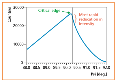
Figure 4. Sample irradiation and observed length limited by incident beam optics
Axial divergence and the use of crossed slits
Rotation of ψ sets the angle of grazing incidence, the amount by which the X-rays spread around this angle depends upon the axial divergence of the beam. Optical components which control the axial divergence are necessary, for example: Soller slits and crossed slits.
Irradiated length
Because of the low angle of incidence, the irradiated length can be very long (more than 10 mm). However, in order to make good measurements it is good practice to ensure that the observed length (that is “seen” by the detector) closely matches the irradiated length. The observed length is determined by the diffracted beam module.
Observation of texture in Co films
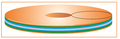
In the production of hard disk, highly textured, hexagonal phase, Co-based magnetic thin films (typically 25 nm thick) are grown over a layer AI/NiP/Cr substrate. A 32 mm diameter circular sample was cut out from a production hard disk.
In this example results from the in-plane diffraction geometry are compared with measurements in the Bragg-Brentano parafocusing geometry.
Figure 5. Showing where the sample was cut from the hard disk
Bragg-Brentano diffraction
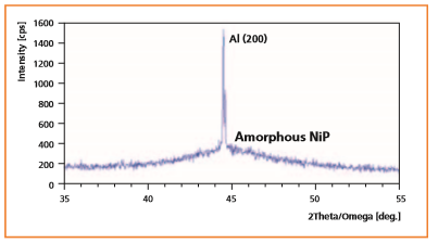
In the Bragg-Brentano geometry, lattice planes parallel to the sample surface are measured. Figure 6 shows a scan taken in this geometry. In this measurements no information from the Co thin film could be obtained. In the range between range between 38° and 47° 2θ) are easily lost under the stronger AI peak and the amorphous NiP scatter from the substrate.
Figure 6. Bragg-Brentano scan
In-plane diffraction
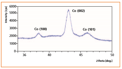
The experiment was repeated in the in-plane diffraction geometry. In measurements in the in-plane diffraction geometry information can be obtained about the surface layers. The optical configuration used in this experimental is described in the section Instrumentation. Figure 7 shows a scan taken in the in-plane geometry on the hard disk. Peaks from the Co (100), (002), (101) scattering planes are revealed. Because the layer is polycrystalline, this scan was obtained without rotating the sample around the axis. However it was believed that the crystal grains have a strong in-plane texture. This was investigated by rotating the sample fully around the axis.
Figure 7. 20 scan using in-plane geometry showing the peaks associated with the Co layer
Bragg-Brentano
The standard diffraction experiment in the Bragg-Bretano geometry was performed on an X’Pert3 MRD system with:
In-plane diffraction
The in-plane diffraction experiment was performed on an X’Pert3 MRD system configured for in-plane diffraction (see Figure 8) with:
Figure 8. Optical set-up for in-plane diffraction
In this experiment the detector 2θ position is set to collect scattering from the (002) reflection. The sample is scanned in φ. The φ scan in Figure 9 shows that there is a strong variation in scattering intensity with sample rotation. The sample was large enough that the complete incident X- ray beam was accepted by the sample during the measurement. Therefore all of this intensity variation could be attributed to texture. For a small sample it may be necessary to account for variation in intensity due to changes in irradiated length on the sample surface.
Figure 9. φ scan showing intensity variation attribute to texture
Reciprocal space maps of single crystal GaN on sapphire
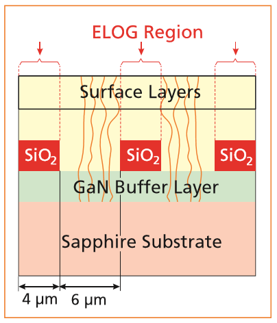
Epitaxial lateral overgrowth (ELOG) has been used to grow striped regions of defect free GaN on sapphire substrates. The structure is shown schematically in Figure 10. SiO2 stripes are deposited on a GaN buffer layer on a sapphire substrate. Further GaN growth then occurs initially from the GaN buffer layer. Defects from the buffer layer continue to propagate through the layer. When the GaN thickness exceeds the height of the SiO2 stripes it also grows laterally across the top of the SiO2, the defects do not propagate laterally. In this way a defect free region is formed over the SiO2 stripes. With in-plane diffraction, the effect of this structure on the GaN in the surface region can be examined.
Figure 10. Representation of the ELOG structure
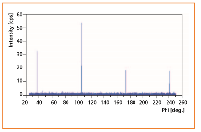
After alignment of the sample in ω, an open detector is set to the 2θ position of the required Bragg reflection. Because the sample is a single crystal it must be scanned carefully in φ in order to find the correct orientation for the reflection. Figure 11 shows an example of a φ scan to find the {10-10} reflections.
Figure 11. φ scan showing the orientation of the reflection
The in-plane diffraction experiment was performed on an X’Pert3 MRD system with:
Figure 12. Optical setup for high resolution in-plane diffraction
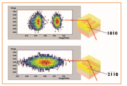
It was found that one of the {2-1-10} planes ran parallel to the SiO2 stripes and one set of the {10-10} planes ran perpendicular to the stripes. High resolution reciprocal space maps (ω/2θ versus ω) were obtained for the (10-10) and (2-1-10) reflections (see Figure 13).
The diffraction spots from the planes running perpendicular to the stripes are broken into two distinct spots corresponding to regions with different (10-10) plane spacings. It is reasonable to suppose that these indicate differences in the strains in the GaN over the SiO2 from that of the GaN between the SiO2 stripes.
Figure 13. Top: 2-axes scan of (10-10) planes running perpendicular to the ELOG region. Bottom: 2-axes scan of (2-1-10) planes running parallel to the ELOG region
The design of the experiment and the form of the collected data will depend upon the nature of the thin film under investigation and how much is already known about the chemistry and microstructure of the film.
Some general ideas for the solutions that can be obtained using in-plane diffraction are summarized here.