
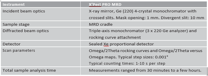
The X’Pert3 MRD X-ray diffraction system is a versatile tool for studying residual lattice strain in solar cell structures grown on relaxed buffer layers. Offcut structures in the form of single crystal AlGaAs/GaAs multilayers on GaAs and Ge substrate wafers and on Ge-on-Si pseudo-substrates were analyzed.
The physical properties of a single crystal solar energy collecting device are dependent upon the unit cell and thin film structure of the layers that form the device. During growth, the thin film unit cell is constrained to an in-plane lattice parameter provided by the substrate.
The physical properties of a single crystal solar energy collecting device are dependent upon the unit cell and thin film structure of the layers that form the device. During growth, the thin film unit cell is constrained to an in-plane lattice parameter provided by the substrate. This can cause strain in the layers that can be useful or deleterious [1]. An AlGaAs/GaAs device structure can be most easily grown on a GaAs substrate because the device structure has lattice parameters identical to, or very close to the substrate lattice parameter. The same device grown on Ge might be expected to show some strain. But because the Ge lattice parameter is only 0.07% (700 ppm) larger than the GaAs lattice parameter, the strain will be very small. The same device
grown on a Si substrate will experience mismatch strains of about 3% (30,000 ppm). It is not normally possible to grow dislocation-free epitaxial single crystal thin films with mismatch strains in excess of about 2% [1]. However, a relaxed Ge buffer layer, several micrometers thick, can provide a surface lattice parameter that is closer to the optimum substrate lattice parameter, while being supported on a more convenient Si substrate. The large lattice mismatch between the substrate and the buffer layer is accommodated by misfit dislocations.
If a Ge buffer layer is completely relaxed it has the same unit cell dimensions as a Ge substrate wafer. Many buffer layers do not achieve complete relaxation but rather can exhibit in-plane surface lattice parameters that vary by up to 10% from the nominal bulk values.
In this work it was necessary to find out some information about the state of strain of devices grown on different types of substrate. To do this requires very accurate measurement of the unit cell d-spacings in the devices. The sample structures posed some challenges to these measurements. Firstly the samples had to be carefully aligned to account for the offcut in the wafers. Secondly, the dislocation strain- fields in the Ge buffer layer, gave rise to diffuse scatter intensity which masked the signal from the device for all but the (02) reflection.
The X’Pert 3
The physical properties of a single crystal solar energy collecting device are dependent upon the unit cell and thin film structure of the layers that form the device. During growth, the thin film unit cell is constrained to an in-plane lattice parameter provided by the substrate.
High-efficiency solar cells can be based on III-V semiconductor multilayer thin film structures. They are typically grown lattice matched or near lattice matched on GaAs or Ge substrates. Novel “Pseudo- Substrates (PS)” are being developed in which Ge or Si-Ge relaxed buffer layers are grown on Si substrates. This has commercial significance because Si substrates are cheaper and offer the possibility for device integration with existing Si technology.
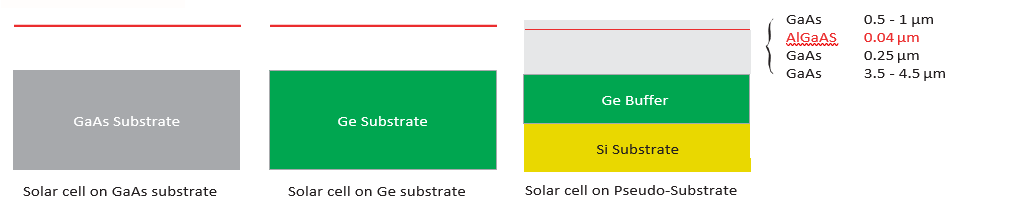
Three samples are described in this report. They all have the same AlGaAs/ GaAs solar cell structure grown on the top. This is a 40 nm AlGaAs well within n- and p-doped GaAs barrier layers all on a GaAs buffer layer. This same structure is grown on three different substrates:
• approximately 3° off 001 GaAs
• approximately 6° off 001 Ge
• Ge buffer layer on approximately 6° off 001 Si
A schematic represention of the samples described is given in Figure 1. The doping levels were below those detectable as lattice strains in GaAs.
Figure 1. Schematic diagrams of sample structures
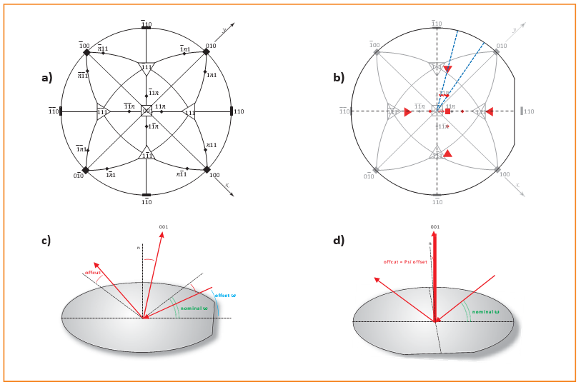
Sometimes epitaxial growth of single crystal thin films can be improved by growing the film on a substrate with a small offcut. “Offcut” describes the misorientation between the surface of the substrate wafer and the closest low index plane (e.g. (001)). Offcut can be visualized by considering the surface normal (n) and the normal to the (001) planes, as represented in a stereo- graphic projection [2].
Figure 2a illustrates the orientations of the primary plane normals for a typical 001 wafer with no offcut. Here the (001) plane normal is coincident with the sample surface normal. The normals to the (100), (010) and (110)-type planes are parallel to the sample surface. The other labelled plane normals such as {111} and {11n} are inclined at angles between these two extremes. Note that pairs such as (11n) and (111) lie along the same azimuth as (110).
Figure 2b illustrates what happens to some of these plane normals if the wafer has some “offcut” in the direction of a major low index azimuth. In this case the plane normals that were originally along this azimuth stay on the same azimuth but are rotated by the magnitude of the offcut. However, the plane normals that were not on this azimuth are rotated and are no longer to be found along the same azimuth as is indicated by the blue dashed lines. (For XRD measurements the azimuth is aligned by the Phi rotation.)
The (00n) type reflection can be most conveniently measured at the Phi azimuths where the offcut angle is accounted for as an offset in either Psi or Omega. Once found, this offset can also be used to find the (nnn) and (11n)- type reflections that lie on the same azimuth as the offcut. Reflections from planes whose normals are not on the azimuth containing the offcut are difficult to find and difficult to analyze.
Figure 2c illustrates the case where the incident and diffracted beams (red arrows) are in the same azimuth as the offcut. In this case the effect of the offcut is to reduce the value of Omega (if the sample is rotated by 180° the Omega value will be increased by the same amount). Figure 2d illustrates the case where the incident and diffracted beams (red arrows) are at 90° to the azimuth of the offcut. In this case the reflection will be found by maintaining the nominal value of Omega and incorporating the offcut value as an offset in Psi.
Note that in both cases the same reflection is being measured. In some cases the offcut may be sufficient to bring another plane normal, e.g. (117), close to the surface normal, thus providing a new surface symmetric reflection [3].
Figure 2a-d. Schematic diagrams of sample offcut. a) (001) wafer based on a stereographic projection to show no offcut. b) Effect of offcut on (001) wafer in the direction of [110] on major plane normals. c) When offset in Omega is required: the incident and diffracted beam are in the same direction as the offcut. d) When offset in Psi is required: the incident beam and diffracted beam are at 90° to the azimuth of the offcut.
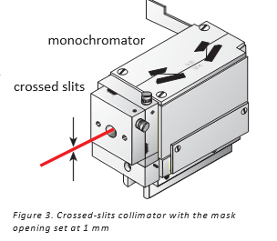
For the measurements, crossed slits, with the mask opening set at 1 mm, were used at the exit of the incident beam monochromator (Figure 3). The crossed slits are used to reduce the axial divergence. This sharpens the peaks that are used in the Psi and Phi alignment.
Using a triple bounce analyzer (TA optics), the 2Theta zero position is checked and calibrated by measuring the position of the straight-through beam (attenuated) with no sample present. The sample is then introduced and positioned so that it cuts the intensity down to about 10% of the maximum value. An Omega scan is performed where the position of the peak intensity of the direct beam is calibrated as Omega = 0°. The sample height is re-positioned in Z so that it cuts the intensity to half the maximum value at Omega = 0°.
The precise peak position may be obtained by collecting a reciprocal space map (2Theta/Omega versus Omega) over a small range and with a small step size (e.g. 0.001° 2Theta), using TA optics. Alternatively a 2Theta/Omega scan using TA optics, over the peak may be sufficient.
It can be useful to measure the peak at a number of different azimuths, for example the azimuths with the offcut incorporated as +Psi and –Psi and the azimuths with the offcut incorporated as additional +offset and –offset in the Omega value. These scans can be compared (e.g. by plotting them together in 2Theta/Omega view). For these samples, this error was investigated and found to be negligible.
Figure 3. Crossed-slots collimator with the mask opening set at 1 mm
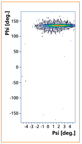
Using an open detector (rocking curve attachment) the 2Theta position is set to the nominal value (e.g. as provided in the data collector) for the reflection (hkl) to be measured. The Omega value is set to its nominal value (for symmetrical reflections this is exactly half of 2Theta). If the offcut is known, then Psi is set to the offcut value and Phi to the appropriate azimuth. A small Phi- Psi map may be measured in order to find and optimize the peak position. If the offcut is not known then a larger Phi-Psi map or pole figure may need to be collected (Figure 4).
Once a peak has been found, the diffracted beam triple-axis monochromator is employed (TA optics) and a 2Theta scan is performed to locate the precise 2Theta position. Having found this the Omega value is set to exactly half this value. Returning back to the open detector (rocking curve attachment), Psi and Phi will again be optimized. This process can be repeated until there are no changes in peak position.
Figure 4. A Psi vs Phi map is collected to identify the peak position.
With the highest resolution setting (triple-axis monochromator), as used here, it is possible to perform very precise measurements of d-spacing on perfect materials such as the GaAs, Ge and Si substrates [4]. These are useful measurements to check the extent of the deviation of the substrate d-spacing from the nominal lattice parameter. In this case the (004) reflection was chosen on account of its high intensity and availability for all substrates.
Two analysis routes are possible using AMASS:
• The 2Theta positions of peaks from scans or maps can be used directly with Bragg’s law to calculate the d- spacing of the lattice planes giving rise to the peak. The peak position can be identified manually or by use of the “Automatic Peak Search” facility. The calculated d-spacing can be displayed in the “Peak Grid”[5,6]. This d-spacing differs from the actual value due to the refractive index effect [7] which is not incorporated in the automatic Bragg’s law calculation. In the examples shown here, this error is approximately -0.005%. It can be compensated by comparing the d-spacings of the substrates with spacings from simulations of substrates rather than with database d-spacings. In this way the refractive index effect is automatically incorporated.
• A 2Theta/Omega scan (or a projected map) can be compared with a dynamical simulation [5,6]. Strain can be added to the substrate in the sample file until the 2Theta values for the simulation and the measurement are the same. The first of these approaches is shown in Figure 5. The peak positions and FWHMs are given in Table 1. The second is used to analyze the device structures on
page 7.
The strain is calculated simply as the difference between the measured and simulated plane spacing divided by the simulated plane spacing.
This corresponds to the strain in the direction of the plane normal. The strains are compared for the different substrates in Table 2.
Table 1. Peak positions and Full Width at Half Maximum (FWHM) for the simulated and measured 004 substrate reflections, shown in Figure 5
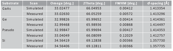
Table 2. Residual strain in the substrates as calculated from the peak maximum positions given in Table 1
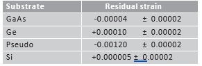
Figure 5. 004 TA Omega/2Theta scans over the substrate peaks. From top to bottom: GaAs , Ge, Pseudo- Substrate and Si (supporting the Pseudo-Substrate). The blue curves are the measured scans, the red curves are the simulated scans. The positions of the peak maxima of the 004 substrate reflections for both the measured and the simulated scans can be found in Table 1
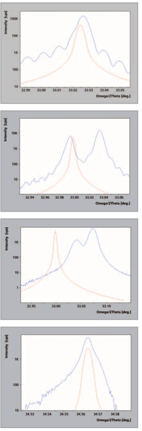
Figure 6. Composition and relaxation are calculated using both the 004 and 444 reflections along the azimuth containing the offcut. Copies of the maps are inset in zoom mode.
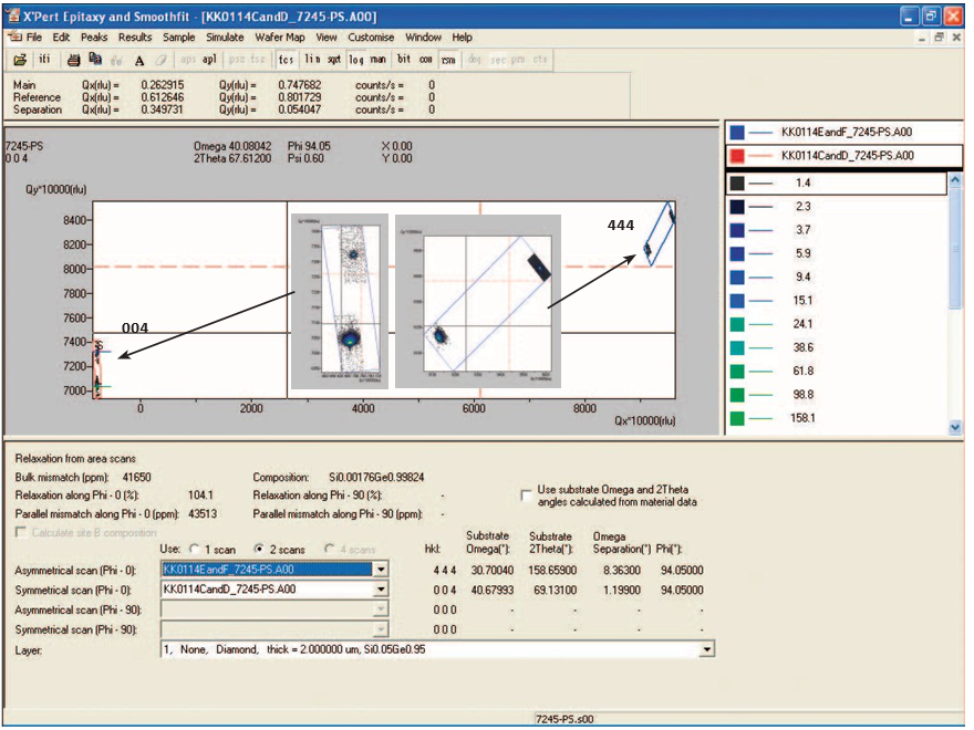
AMASS can take the peak positions obtained from surface symmetric and asymmetric reflections (scans or maps) and use them to calculate the composition and relaxation of a buffer layer. These calculations assume that there is no substrate offcut. Included in these calculations is the simplification that the unit cells of the layers are either regular cubic or tetragonal and that they are not deformed by shear strains. The type of deformation that a cubic or tetragonal unit cell (for a strained layer) undergoes when it is grown on an offcut sample is not so predictable. AMASS calculations applied to offcut layers provide an approximate guide as to the state of the layers, but the errors in applying these calculations to the layers are unknown and the user should be aware that this is the case. Figure 6 shows an example of the relaxation and composition analysis using AMASS. The maps were collected with the offcut as an offset in Omega. (It is not possible to collect an asymmetric map along the azimuth perpendicular to the offcut. See Figure 2b). In the sample file the layer was described as a SixGe(1-x) layer. The analysis gave the composition, within error, to be 100% Ge and the relaxation, within error, to be 100%. Given this information the peak position of the Pseudo-Substrate (previous page) was then compared with the simulated position of a pure Ge substrate for a more precise measurement of strain.
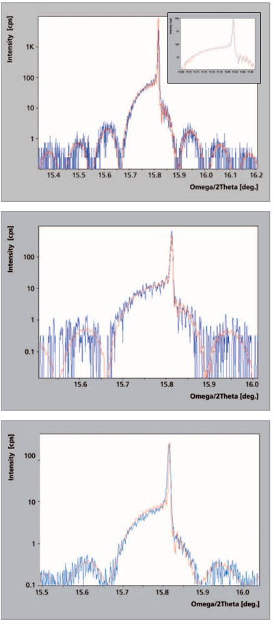
The solar cell device structures are clearly revealed using the 002 reflection because this reflection is forbidden to Ge and Si. It is also more sensitive to compositional variations than the 004 reflection and hence reveals the AlGaAs single well more clearly. In all cases the 002 reflections were obtained for the condition in which the offcut was accommodated in Psi.
For the device grown lattice matched to GaAs the profile was of a very good quality. For the device grown on Ge the simulation was made easier by the absence of the Ge substrate peak which is very close to the GaAs peaks. For the device on the relaxed Ge-on-Si Pseudo- Substrate, this was the only reflection for which it was possible to see the scattering from the device, as it was otherwise lost in the diffuse scattering from the relaxed Ge buffer layer.
Sample files were created using the full sample structure and were used to simulate the 002 reflection. These were compared with the measured data and modified, either manually or via fitting until a best fit was obtained. The nominal device parameters for thickness and composition fitted the data well. In each case it was necessary to introduce a strain to the device layers in order to shift the position of the main GaAs peak. The results for this strain are given in Table 3.
Table 3. Residual strain in the solar cell devices, grown on different substrates, as resulting from the best fit simulations, shown in Figure 7
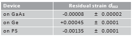
Figure 7. Best fit simulations of 002 reflections from top to bottom: device on GaAs substrate with zoom inset, device on Ge substrate and device on Pseudo-Substrate
This application report describes some of the approaches that can be made to begin to examine the strain in solar cell devices grown on a variety of offcut substrates.
The raw data provide unit cell d-spacings which are then formulated as strains i.e. relative departures from the expected d-spacing of the unstrained crystal. The tailored solutions provided in AMASS for device simulation can be applied to the data for symmetric reflections where the offcut is either known and entered into the simulation parameters (in the case of Omega offset) or is not present in the profile via a Psi offset. The solution provided in AMASS for calculation of composition and relaxation of buffer layers can be applied as a rough guide only for the azimuth containing the offcut.
There are many paths that can be taken to relate these results to device properties as measured by other physical means. The complete measurement of the full strain tensor for the crystal would require several measurements of different d-spacings along different azimuths. Certainly it is possible using high-resolution optics and a well calibrated 2Theta zero position, to measure the d-s pacings to a high accuracy. The offcut affects the orientation of all the planes and needs to be characterized at the start of the project. This can be most easily done with the use of a large Phi vs Psi map to find the (00n) reflection. The effect of the offcut on plane normals which are not contained in the same azimuth can be best understood by the use of the stereographic projection.
The rotation of the crystal due to the offcut results in a displacement of the off-axis plane normals from standard azimuths. Full alignment and analysis of reflections whose normals are not in the same azimuth as the offcut requires advanced treatment beyond that presented here.