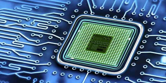
Semiconductores compuestos
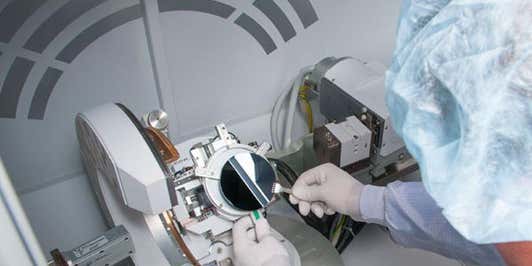
Metrología de película delgada para semiconductores compuestos
Semiconductor solutions to help connect us to the world

Our physical, chemical, and structural analysis solutions for semiconductors cover the entire value chain. With them, you’ll be able to:


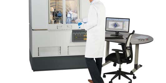
From phones and laptops to cars and smart meters – so many of the devices we rely on contain advanced electronics and semiconductors. While manufacturing multi-layered structures, it is essential to control your film parameters and our X-Ray instruments and expertise help carry out the detailed analysis you need for this.
As well as digital devices, semiconductors can enable several sustainable technologies, such as LED lighting and more efficient batteries. Read our blog to discover how our X-ray analysis solutions can help you contribute to this sustainable future.
Check out our article on compound semiconductors to learn about today’s semiconductor landscape, what the future holds, and how we can help you keep up with all these developments.
We’d love to hear about your challenges and discuss how we can help you solve them. Reach out to us and one of our experts will be in touch for a chat.