In this application note, we studied the effects of thermal annealing on the structure of multiple quantum wells. From reciprocal space maps collected on an X’Pert3 MRD system equipped with a nonambient chamber, information about structure, composition and disordering could be derived.
Fast X-ray measurements are especially required for monitoring of physical processes with rapidly changing parameters. They can be used to measure the structural properties of materials used in semiconductors, including attractive wurtzite type gallium nitride.
Fast X-ray measurements are especially required for monitoring of physical processes with rapidly changing parameters. They can be used to measure the structural properties of materials used in semiconductors, including attractive wurtzite type gallium nitride. As just one example, the in situ and real-time X-ray characterization of InGaN/GaN multiple quantum wells (MQWs) during thermal annealing is demonstrated.
Accurate control of semiconductor layers has enabled designers to reproduce the one-dimensional ‘particle in a box’ structure that is commonly used to explain Schrödinger’s equation. Thin alternating layers of (for example) InGaN and GaN can produce devices like quantum well lasers, which have remarkable optoelectronic properties. Electrons are here confined to a single dimension, perpendicular to the layers themselves, and free to move in the other two. The discontinuities in the conduction band at the join between the different materials produce an offset, and if this is large enough, the electrons are confined to the material with the narrower band gap (InGaN). A MQW structure comprises more than one well. It has a larger volume of the active region and thus allows for higher light powers. Structures are often processed by MBE (Molecular Beam Epitaxy) or MOCVD (Metal Organic Chemical Vapor
Deposition). Different layer thicknesses, compositions, and values of doping and strain give devices with different electronic and optical properties. Crystal quality is however critical to device operation and efficiency, and particularly during process steps like thermal annealing. In the present work, we describe the X-ray analysis of the InGaN/GaN multiple quantum wells during thermal annealing in situ and with high time resolution (real-time). The measurements showed compositional disordering of quantum wells starting after 30 minutes annealing at 800 °C and resulting in completely disordered MQWs.
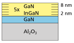
The sample was an InGaN/GaN multiple quantum wells structure consisting of five periods of InGaN (well) and GaN (barrier) layers deposited on a GaN buffer. The sketch of the vertical structure of the sample is schematically illustrated in Figure 1.
The intensity distribution of the MQW in reciprocal space (the reciprocal space map, RSM) was measured around the asymmetrical (11-24) reflection of GaN. The X’Celerator was switched to the receiving slit mode (full active length) before adjusting the maximum GaN intensity of the main GaN (11-24) peak.
Figure 1. Sketch of the InGaN/GaN multiple quantum wells structure used for the annealing experiment
The configuration of the X’Pert3 MRD used for the reciprocal space mapping measurements during the thermal annealing experiments is described in Table 1. The RSMs were thus measured as combinations of static 2θ scans for different ω positions of the sample. The measurement time for each RSM was 20 minutes, which is about a factor of 2 lower than for the X’Celerator detector in scanning operation mode. The measurement time with a proportional detector would exceed 3 hours.
Figure 2 shows the RSM measured at room temperature. The superlattice peaks deviate from the GaN peak position in a direction parallel to the sample surface. This indicates a tilt of about 10 arc seconds for the MQW structure with respect to the GaN buffer. The interpretation of such RSM is well known [1, 2]. The positions of the main reflections correspond to a periodicity D = 10.2 ± 0.5 nm (sum of barrier and well layer thicknesses) and to a composition x = 0.235 ± 0.003 of the InGaN active layer. The composition of the active InGaN layer was calculated assuming that InGaN and GaN layer thicknesses in a stack are as expected from the growth procedure (8 nm and 2 nm for the GaN and InGaN layers, respectively).
Table 1. Configuration of the X’Pert3 MRD system used for the measurements of the reciprocal space maps
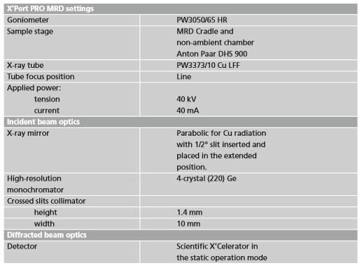
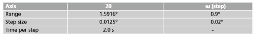
Table 2. Scan settings used for the reciprocal space mapping measurements
The sample was annealed under normal atmospheric pressure, from room temperature to 800 °C in 50 °C steps using the DHS 900 Domed Hot Stage developed by Anton Paar GmbH, Austria. At each step, the temperature of the sample was stabilized for
10 minutes, then the main GaN peak was aligned and the reciprocal space map was collected. The ratio of the SL0 peak intensity to its value at room temperature was evaluated to monitor structural changes. The SL0 peak represents the average lattice parameter of the MQW structure.
Figure 3 shows this ratio as a function of the temperature. Below 800 °C, there is only a small drop in the variation of the intensity ratio. This is caused mainly by the changes of the scattering factors. After 30 minutes annealing at 800 °C, the intensity ratio clearly started to fall, and decreased about five times after 50 minutes. The intensity of the GaN peak, however, decreased by only 40% because of the change of the scattering factor.
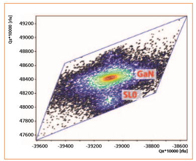
Figure 4 shows the RSM measured after 50 minutes of annealing at 800 °C. The SL+1 superlattice peak disappeared, leaving only the weak peak at the position of the SL0 reflection. This indicates that the annealing process resulted in a complete compositional disordering of the quantum wells.
Figure 2. Intensity distribution in reciprocal space measured on the InGaN/GaN multiple quantum wells structure at room temperature. Using the X’Celerator detector, the periodicity and In molar fraction are available in 20 minutes
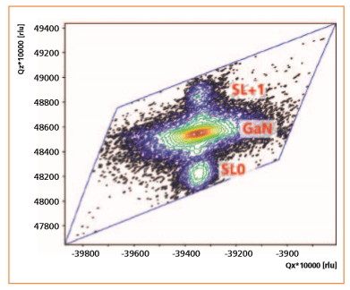
Figure 3. Decrease of the SL0 peak intensity versus annealing temperature. Compositional disordering of MQWs started at 800 °C. The intensities are normalized to the intensity measured at room temperature
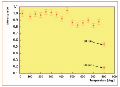
Figure 4. Intensity distribution in reciprocal space measured on the InGaN/GaN multiple quantum wells structure after 50 minutes annealing at 800 °C
The X’Pert3 MRD equipped with an X’Celerator detector is ideal for performing fast reciprocal space mapping to characterize semiconductor structures. Extended with an Anton Paar DHS 900 Domed Hot Stage, it was successfully used to study the thermal stability of the wurtzite type InGaN/ GaN MQW.