With the new edition of the data collector software large reciprocal space maps can be measured with PIXcel3D detector within tens of seconds. This option, combined with the functionality of the domed heating and cooling stages (DHS 1100 and DCS 350), enables in situ monitoring of temperature effects on the epitaxial layers in real time.
In this application note, the results of the X-ray analysis on the thermal stability of an AlInN/AlN/GaN heterostructure is demonstrated. By using a PIXcel3D detector, reciprocal space maps (RSM) were rapidly measured while annealing the sample at 600˚C. The timeresolved data allowed to monitor the degradation process and its kinetics.
A lot of research effort is currently spent on the development and improvement of gallium nitride (GaN) based high electron mobility transistor (HEMT) structures. Due to the physical properties of the wide band gap nitride materials, a greatly increased power density is feasible compared to established technologies resulting in smaller transistors with higher output power for high-frequency applications.
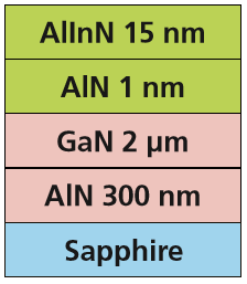
The sample was grown by MOVPE on a 2 inch c-plane sapphire substrate, starting with a high-temperature AlN (300 nm) layer on an AlN nucleation layer followed by a GaN (2 µm) buffer layer. On top of the GaN buffer a thin, 1 nm AlN spacer layer and 15nm Al0.84In0.16N barrier layer were deposited. A sketch of the vertical structure of the sample is schematically illustrated in Figure 1.
Figure 1. Sketch of the AlInN/AlN/GaN HEMT structure used for the annealing experiment
A typical HEMT structure consists of a stack of two semiconductor layers with different energy band gaps, for instance AlInN on GaN. At the interface a very low resistivity channel is formed for confined electrons with ‘high electron mobility’ - the so-called two- dimensional electron gas. An applied voltage via a gate electrode controls the conductivity of this layer. The layers are typically grown epitaxial by MBE (molecular beam epitaxy) or MOVPE (metal organic vapor phase epitaxy). These techniques enable an accurate control of the materials chemistry and interface quality. Since the structural quality of the layers and their interface is critical for the device performance, detailed knowledge of the effects of further process steps, like thermal annealing, on these parameters is crucial.
The following configuration of the X’Pert3 MRD was used for the measurements
The RSMs were measured as 2-axes scans with the PIXcel3D in static 1D mode. The following scan settings were employed:
The intensity distribution of the heterostructure in reciprocal space (the reciprocal space map, RSM) was measured around the asymmetrical grazing exit (20.4) reflection of GaN and AlInN. Additionally (00.2) ω-2θ pattern were recorded in the vicinity of the GaN Bragg peak. The PIXcel3D detector was electronically switched between the receiving slit mode for the line scans and 1D static mode for the RSM. In the former mode the active length varied between full (14 mm) for the alignment steps and 1 mm for the line scans. In the case of RSM measurements, the ‘static’ mode records a fixed 2θ range of 2.51º while the ω position is varied. Both measurements, a (20.4) RSM and a (00.2) line scan were completed within a total time of 15 minutes. The sample was annealed under normal atmospheric pressure for 150 minutes at 600°C using Anton Paar’s DHS 900 Domed Hot Stage.
Figure 2. Intensity distribution in reciprocal space measured on the AlInN/AlN/GaN heterostructure at 600°C. Using the PIXcel detector, the mismatch and In molar fraction are available in 15 minutes.
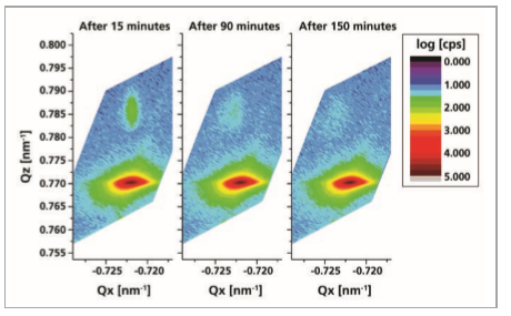
Figure 2 shows the reciprocal space map data measured during annealing at 600ºC. The matching Qx values in the left RSM verify pseudomorphic Al1-xInxN and the indium content is calculated to x=0.16 while clear changes are visible in the middle and right graph of Figure 2. The intensity of the Al1-xInxN layer peak dropped significantly during the annealing. At the same time the center of its reciprocal lattice distribution shifted, (corresponds to a change in interatomic spacing) while the GaN peak remained unchanged. Both observations indicate that the annealing process resulted in a relaxation of the lattice accompanied by the generation of defects. The observed final position corresponds to a relaxation of the lattice of about 80%. This affects the crystalline quality of the layer and the coherence of the critical heterostructure interface.
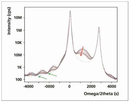
The diffraction pattern of the line scans exhibits an increasing deterioration of the AlInN barrier layer with an exponential drop-off of the corresponding diffraction peak intensity and a change in peak position as indicated by the red arrow in Figure 3.
The drift of the measured peak position is attributed to relaxation by misfit dislocations or diffusion. The layer thickness, measured by the peak fringe distance (green arrows), is constant until the fringes vanish. After further annealing for 1h at 700°C (dashed line), the pattern shows no traces of an AlInN peak or its fringes.
Figure 3. Evolution of the AlInN (00.2) peak intensity at 600°C versus annealing time. Clearly the thickness is not influenced as the green arrows indicate the constant peak fringe distance. The dashed line is recorded after 1 h annealing at 700°C and is taken as an equilibrium reference
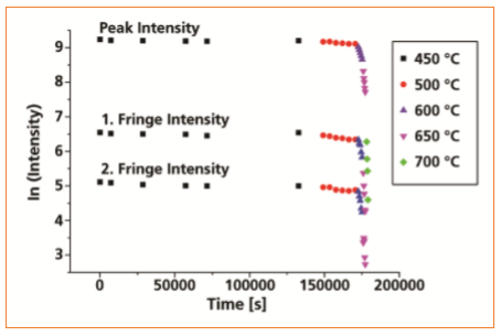
The slope of the exponential drop-off of the AlInN peak intensity as seen from the semi-log plot in Figure 4 (left) provides information about the kinetics of the decomposition of the material. Here, an identical structure has been annealed at different temperatures yielding a strongly temperature- dependent exponential intensity degradation over time. A detailed evaluation is subject to publication and would exceed the given frame here.
Figure 4. Decrease of the (00.2) AlInN peak and fringe intensities versus annealing time for different temperatures (data acquired in a second iteration with an identical structure)
The thermal stability of a wurtzite type AlInN/AlN/GaN heterostructure for high-power RF applications was successfully studied in an Anton Paar DHS 900 Domed Hot Stage. For this purpose reciprocal space maps on one asymmetric reflection (20.4) and ω/2θ scans around a symmetric reflection (00.2) were measured by means of the PIXcel3D detector. This data was employed to evaluate the development of lattice strain and crystal fidelity as a function of time and temperature. The unique 0D and 1D features of the detector allowed to collect both data sets rapidly and in a straightforward manner.