Metrology solutions for bulk and thin film-based electronic components manufacturing

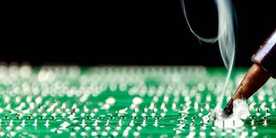
Single-crystal substrate materials with carefully controlled composition and crystal orientation are at the heart of semiconductor manufacturing. The thin film structures created on these substrates are then shaped by sophisticated processes into intricate devices on a wafer. Typical materials involved in advanced thin film devices are semiconductors, metal alloys, dielectrics, oxides, and polymers. This mandates accurate monitoring and control of substrate, thin film and device manufacturing using multiple metrology techniques. Equally important is the fine control over the process materials, for example CMP slurries and plating solutions.
Single crystal substrate manufacturing involves seeding, crystal growth, grinding, cutting, polishing and final control. Throughout all these steps, quick and precise crystal orientation control is critically important to ensure cost efficient production of high-quality substrates.
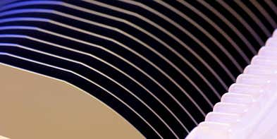
These substrates are the foundation for the thin film-based devices, which are manufactured using a complex multistep fabrication process. X-ray fluorescence (XRF) or X-ray diffraction (XRD) are an integral part of any such manufacturing process to monitor and control critical thin film parameters at every step.
In a different process flow, electronic displays employ various technologies such as liquid crystals, pigment dispersions, quantum dots, and OLEDs. In most of these, the particle size and shape play an important role and count on our particle characterization range for reliable characterization. For OLEDs, we provide strict control over the polymer characteristics such as size and molecular weight which is paramount to the display quality.
Malvern Panalytical is closely associated with the electronics industry with a wide range of solutions across the entire value chain: