Thin film metrology
X-ray thin film analysis


X-ray thin film analysis
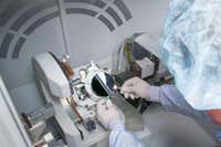
X-ray metrology is the ideal tool for thin film analysis in the development and mass production of different kind of layer-structured micro- and optoelectronic devices.
X-ray metrology techniques have kept up with the progress in the industry through the development of new layer-based applications and technologies.
They continue to serve as essential tools from the R&D phase through pilot production to full-scale automated manufacturing of semiconductor devices.
Measurement tools based on X-ray methods, such as XRD, XRR and XRF, have proven to provide rapid, non-destructive, reliable and accurate access to critical thin film parameters ranging from ultra-thin single layers to complex multilayer stacks.
Find out more about our thin film analysis instruments below.
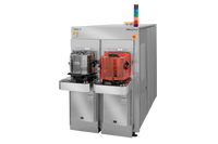
High end floor-standing WDXRF spectrometers
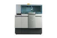
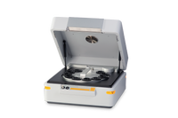
High throughput simultaneous WDXRF spectrometer
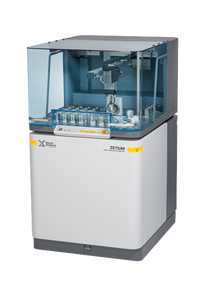
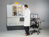
Advanced semiconductor thin film metrology solution
Fast and accurate at-line elemental analysis
Versatile research & development XRD system
Versatile research, development & quality control XRD system