Thermal Stability of Gallium Nitride based high electron mobility transistor structures
Application note
Thin film metrology for compound semiconductors

The increasing market demand for high-performing (opto)-electronic, high-power, high-frequency devices is driving today’s compound semiconductor industry to address new challenges. GaN and SiC are the materials of choice for high-power electronics. GaAs- based Vertical-Cavity Surface-Emitting Lasers (VCSELs) are widely used for facial recognition in mobile phones, while GaN technology has revolutionized LED lighting and high-frequency HEMT devices.
Innovations like thin crystalline films with tailored optical and electrical properties, the continuous improvement of high-volume production processes, and enhanced quality management are all necessary to increase the yield and control the costs of producing such devices. This is where X-ray metrology is an ideal, proven tool to help the industry realize these goals efficiently.
Metrology tools based on X-ray techniques (XRD, XRR, and XRF) have been proven to be reliable and powerful. No other technique offers the unique combination of benefits that X-ray techniques provide non-destructive measurement, accuracy, precision, and absolute analysis for the ex-situ investigation of epitaxial layers, heterostructures, and superlattice systems.
Malvern Panalytical has worked in close collaboration with the compound semiconductor industry since its early beginnings to establish XRD and XRF as industry-standard metrology tools. This long experience means that we understand our customers and their analytical problems, enabling us to offer efficient and automated control solutions for applications from R&D to volume semiconductor production.
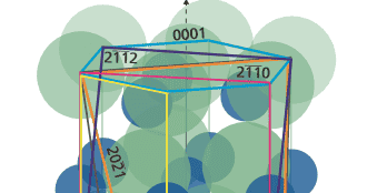
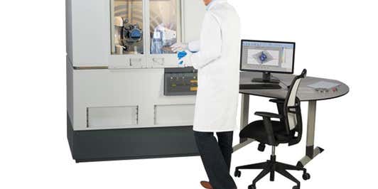
X'Pert3 (X'Pert3 MRD and X'Pert3 MRD XL) is an XRD platform for high-resolution rocking curve, X-ray reflectivity, and ultrafast reciprocal map (URSM) analysis. It provides absolute and accurate information on crystal growth parameters such as material composition, film thickness, grading profile, phase, and interface quality. Crystalline quality parameters such as mosaicity and defect density can also be estimated from such measurements. In addition, an MRD platform can also be used for high-resolution topographic imaging of defects in substrates and thin films. The instrument fits in research and production environments combined with automatic wafer loading.
Crystal Orientation Range
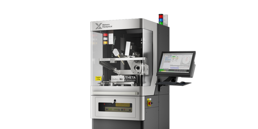
Our new high-speed crystal orientation range makes use of Azimuthal-scan technology to determine the crystal lattice orientation and more, returning accurate results in as fast as ten seconds. Able to characterize a wide range of materials, the SDCOM and DDCOM benchtops deliver high speed without compromising accuracy, while the Omega/Theta offers the highest accuracy and flexibility. The other solutions part of the crystal orientation range are meant for high operational capacity while being able to smoothly integrate into your existing systems. The Wafer XRD 200 and Wafer XRD 300 enable high throughput screening with advanced sorting options for wafer end control while the XRD-OEM tool provides an integrated solution for in-line crystal orientation directly inside crystal processing devices such grinders and wire saws.
XRF (2830 ZT) gives thickness and composition information for a wide range of thin films, with contamination and dopant levels and surface uniformity. It can analyze thicknesses down to half an atomic layer.