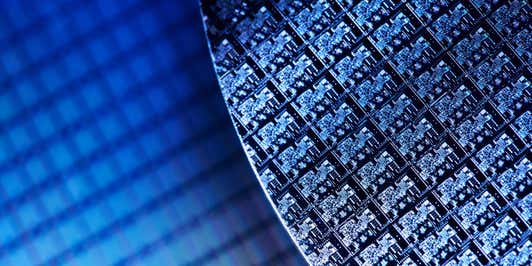
Semiconductor metrology


Precision and quality are keywords in the semiconductor industry, a field that finds usage in every environment of today’s world. Semiconductor metrology refers to steps and practices that are being implemented in the area for the measurement and characterization of the physical and electrical properties of semiconductor devices and materials. Accurate dimensions and metrology determined by measurement results have been the key factors thus far for production processes with low tolerances and high performances.
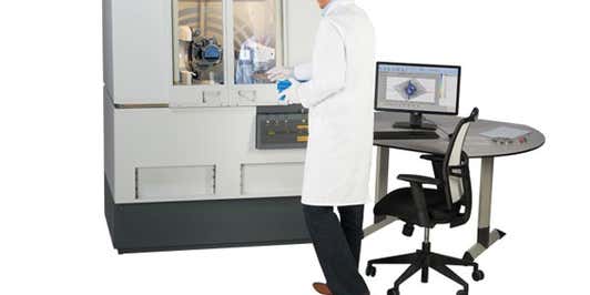
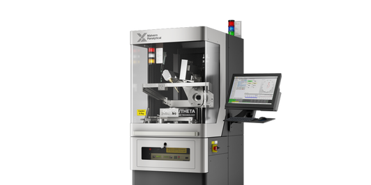
Malvern Panalytical offers a range of advanced x-ray metrology solutions, tools, and technologies developed with the goal of supporting various stages of semiconductor manufacturing with non-destructive measurements, from material characterization to wafer inspection.
As previously established, Metrology plays a vital role in the semiconductor industry, by providing essential material characterization, measurements, and analyses.
As this industry continues to evolve with galloping steps, providing structural and chemical properties becomes increasingly critical in several key areas:
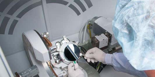
Wafer inspection refers to the process by which semiconductor wafers are structurally and chemically checked for defects, irregularities and inhomogeneities. This way any problems can be found long before the functional tests on the final device. Wafer inspection with x-ray metrology is often used to measure the following properties:
Controlling these properties is critical to fabricating functional devices within their design specifications. Early detection enhances yield and saves time and resources in the long-term perspective.
Over the years, Malvern Panalytical has continued to provide its customers with high throughput and best-in-class solutions to support the ever-changing and ever-tightening process requirements in the semiconductor industry.
Malvern Panalytical is closely associated with the electronics industry with a wide range of solutions across the entire value chain: