Silicon semiconductors
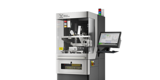
In-line thin film metrology solutions for semiconductor manufacturing process optimization


In-line thin film metrology solutions for semiconductor manufacturing process optimization
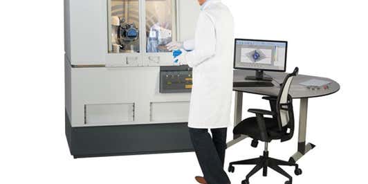
Electronics industries has rapidly advanced on the back of silicon SEMI, data storage, RAM, IC, and RF filter technology over the years, and the rate of change continues to follow Moore’s law. These small devices are at the heart of many advanced functional gadgets used in communication, PCs, consumer electronics, automotive, and advanced electronics for medical, industrial, and government applications. Most of these devices employ multiple layers of thin film on silicon wafer substrates. X-ray wafer metrology tools are an integral part of any silicon SEMI fab to monitor and control critical device parameters.
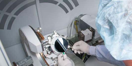
Typical materials used in these advanced thin-film devices are semiconductors, metal alloys, dielectrics, and polymers with thickness ranging from several microns down to monolayers. To understand, improve, and design new devices, it is essential to measure key thin film properties such as layer thickness, crystallographic phase, and alloy composition, strain, crystallinity, density, and interface morphology at every stage of the multi-step fabrication process. This presents considerable challenges to X-ray metrology techniques used to control the manufacturing process – instrumentation must keep pace with developments and meet increasingly rigorous semiconductor wafer metrology demands.
Instrument performance is one of the key aspects of improving yield and product quality in semiconductor manufacturing. Over the years, Malvern Panalytical has continued to provide its customers with high throughput and best-in-class solutions to support the ever-changing and ever-tightening process requirements in thin-film analysis.